
Printed Circuit Boards
From a complex multi-layer board to a double sided surface mount design, our goal is to provide you a quality product that meets your requirements and is the most cost effective to manufacture. Our experience in IPC Class III standards, very stringent cleanliness requirements, heavy copper, and production tolerances allow us to provide our customers exactly what they need for their end product.
Estimated Prototype Delivery 1-5 days
Standar Production 4-6 weeks
| Category | Description | Sym. | Capability |
|---|---|---|---|
1. Microvia Diameter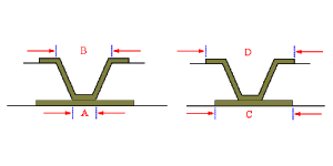 |
1.1 Microvia Diameter at Target Land |
A | 100 um 0.004" |
| 1.2 Microvia Diameter at Capture Land |
B | 125 um 0.005" |
|
| 1.3 Microvia Target Land Size |
C | 0.012" | |
| 1.4 Microvia Target Land Size |
D | 450 um 0.0177" |
|
2. Stagger & Stack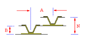 |
2.1 Min. Staggered Via Pitch Staggered Via Pitch |
A | 560 um 0.022" |
| 2.2 RCC Thickness RCC |
B | 50 um 0.002" |
|
| 2.3 Blind Via Layers |
N | 2 | |
3. Material & Construction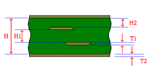 |
3.1 Finished Board Thickness |
H | 0.012" – 0.250" |
| 3.2 Min. Inner Layer Thickness |
H1 | 0.075 mm 0.003" |
|
| 3.3 Min. Dielectric Thickness |
H2 | 0.05 mm 0.002" |
|
| 3.4 Max. Inner Layer Copper |
T1 | 6 oz | |
| 3.5 Max. Outer Layer Copper |
T2 | 6 oz | |
4. Warp |
4.1 Warp & Twist (Max.) |
A B | < 0.75% |
5. Pad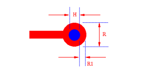 |
5.1 Min. Finish Hole Size |
H | 0.005" |
| 5.2 Min. Land Size |
H | 0.018" | |
| 5.3 Min. Annual Ring for Via |
R1 | IPC Class 2 | |
| 5.4 Min. Annual Ring for Component |
R1 | 0.05 mm 0.002", provided designed per IPC |
|
6. Drill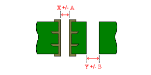 |
6.1 Tolerance for PTH Hole |
A | 0.08 mm 0.003" |
| 6.2 NPTH Hole Tolerance |
B | 0.05 mm 0.002" |
|
7. Registration for S/M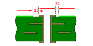 |
7.1 Registration for S/M to Pattern |
S1-S2 | 0.0024" |
| 7.2 Registration for Legend to S/M |
NA | 0.005" | |
8. Registration for Drill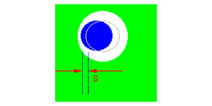 |
8.1 Registration for Drill to Inner Layer |
S | 0.075 mm 0.003" |
| 8.2 Registration for Drill to Datum |
S | 0.05 mm 0.002" |
|
| 8.3 Registration for First Drill to Second Drill |
NA | 0.005" | |
9. Registration for Layers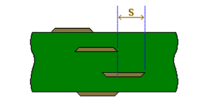 |
9.1 Layer to Layer for 4 layers |
S | 0.08 mm 0.003" |
| 9.2 Layer to Layer for 6 layers |
S | 0.10 mm 0.004" |
|
| 9.3 Layer to Layer for 8 layers |
S | 0.13 mm 0.005" |
|
10. Line Width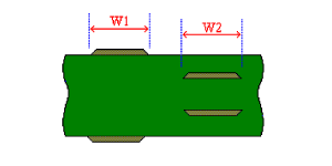 |
10.1 I/L Min. Width (0.5 oz) |
W2 | 0.003" |
| 10.2 O/L Min. Width (0.5 oz) |
W1 | 0.003" | |
11. Line Space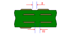 |
11.1 I/L Min. Space |
S2 | 0.003" |
| 11.2 O/L Min. Space (0.5 oz) |
S | 0.003" | |
12. Drill Capability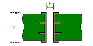 |
12.1 Max. Aspect Ratio (Board Thickness 0.063") |
H/T | 12.0 |
| 12.2 Min. Drill Hole Size (Board Thickness 0.063", After Plating) |
H | 0.0083 | |
13. S/M Thickness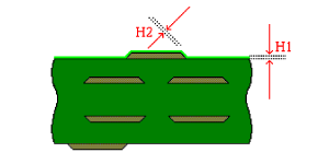 |
13.1 Max. Thickness on Copper |
H1 | 0.025 mm 0.001" |
| 13.2 Max. Thickness at Shoulder |
H2 | 0.0075 mm 0.0003" |
|
14. S/M Capability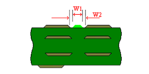 |
14.1 Min. SMD Space for Dam |
W2 | 0.0078" |
| 14.2 Min. Dam Size |
W1 | 0.0004" 0.0005" for white and black colors |
|
15. Carbon Capability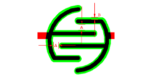 |
15.1 Max. Contact Resistance |
NA | 30 Ω / sq |
| 15.2 Max. Primary Resistance |
NA | 30 Ω | |
| 15.3 Min. Thickness |
NA | 0.0004" | |
| 15.4 Min. Space |
A | 0.015" | |
| 15.5 Max. Space for Registration |
B | 0.007" | |
16. HAL Capability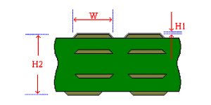 |
16.1 Min. PCB Thickness for HAL |
H2 | 0.6 mm 0.0236" |
| 16.2 Min. Pad Width/Space for HAL |
W | 0.25 mm 0.0098" |
|
| 16.3 HAL Thickness for any point |
H1 | 0.001 mm ~ 0.025 mm 40micro-inch ~0.001" |
|
| 16.4 Thickness on QFP Pad (0.05" Wide Quad) |
A | 0.015 mm ~ 0.030 mm 0.0006" ~0.0012" |
|
17. HAL Capability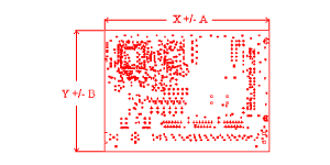 |
17.1 Outline Tolerance-Punching |
AB | NA |
| 17.2 Outline Tolerance-Routing |
AB | 0.005" | |
18. Beveling Capability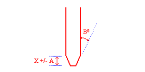 |
18.1 Beveling Angle |
B | 200-600 |
| 18.2 Tolerance for Outline of Bevel |
A | + - 0.005" | |
19. V-Cut Capability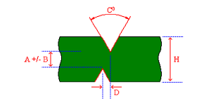 |
19.1 V-Cut Angle V-Cut |
C | 30° |
| 19.2 Range of Board Thickness |
H | 0.030"~0.125" | |
| 19.3 Tolerance of V-Cut Residual |
B | 0.05 mm 0.003" |
|
| 19.4 V-Cut Off Line V-Cut |
D | 0.125 mm 0.005" |
|
20. Test Capability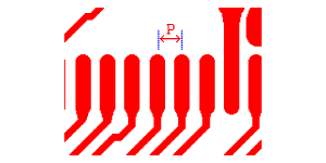 |
20.1 Voltage |
NA | 5 –500 VDC |
| 20.2 Isolation |
NA | 500 MΩ | |
| 20.3 Continuity |
NA | 20Ω~100KΩ | |
| 20.4 Min. SMD PAD Pitch SMD |
P | 0.3 mm 0.0118" |
|
21. Impedance Control Capability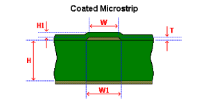 |
21.1 Impedance Control > 50O |
NA | +/- 10% |
| 21.2 Impedance Control < 50O |
NA | +/- 10% | |
22. Differential Impedance Capability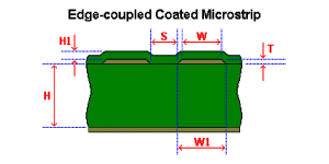 |
22.1 Differential Impedance Control > 50O |
NA | +/- 10% |
| 22.2 Differential Impedance Control < 50O |
NA | +/- 10% | |
23. Coplanar Impedance Capability |
22.1 Coplanar Impedance Control > 50O |
NA | +/- 10% |
| 22.2 Coplanar Impedance Control < 50O |
NA | +/- 10% |
